The electric package has a Raspberry PI 3B+ and a stepper motor drive board. I am using a 555 (on the driver board) to debounce the pushbutton. The interrupt is the discharge pin (7) of the 555 with a 10k pull-up (tied to the 3V rail). The 555 output pin is a 5V signal, which I can not use because the PI GPIO pins are 3V. Which is low when the push button is not depressed and goes high when pressed. So it is this rising edge that triggers the interrupt. I set up the interrupt with the following Python statement.
You can use a voltage divider to convert the 5.0V signal to 3.0V signals so that the different board voltages are compatible. Here is a test simulation via LTspice for the conversion. Notice how the voltages in blue (5.0V) have been converted to the voltage highlighted by the green waveform (3.0V).
Now, looking at that monstrosity of a test jig test setup which is making me feel a bit light headed ova’ heeah’ ( ), there might be an issue with all of those long wires. Please be aware that when you have two circuits separated by long wires, their grounds might not be at the same potential. Can you try shortening the interconnecting wires between the two boards such that they’re much closer together as shown here - can you put the motor board where the blue image is located if not, as close as possible?:
Besides this potential in voltage differences, you also want to make sure that the ground wiring has a strong connection. Preferrably, you should use thicker wire for the ground connections due to the fact that there is in inverse relationship between a voltage drop and the wire thickness. The thinner the wire, the higher its impedance, and vice versa. So, if the wire has a larger cross sectional area, the lower its impedance via this formula: R = p (L / A), where A is the cross sectional area. Also remember that there might be a voltage drop due to this: IR (pronounced as an “eye” “are” drop). Note that the voltage drop is proportional to the length, and the current and inversely proportional to the cross sectional area when you perform the substitution:
V = IR = I x p (L / A))
Thus, you should always try to keep the interconnecting wiring as short as possible and for the ground wiring, make them shorter and larger.
Your picture shows the test jig/setup. Here is a picture of the electronics unit installed (in the blue area shown in your picture). In that new picture, you can also see the PI USB cables.
You’re very right about long wires making a great antenna for all sorts of noise. I shortened the wires when I installed the electronic unit.The drive board has GND planes on both and bottom layers.
I did not think about using a voltage divider to convert the 5.0V signal to 3.0V. I will try that on the next version PCB.
Will resolder all the connections.
Regarding your statement where you stated that when you put pressure on the IO pin with your DVM probe,and observe that the issue goes away. Besides a solder touch up. Also make sure that the wires are crimped correctly. I have come across issues where bad crimping is the source of intermittent or outright no connection. Generally, to test this, you can do an ohm test between a test point on one board and a test point on the other where two points are connected via the mating wires.. It should be zero ohms, of course. Repeat for all mating wires.
Another simple test is to apply pressure on a wire forcing contact prior to and during turn on to see of the issue goes away. Process of elimination as you test all of the mating wires.
I do not think it is a connection problem. I am using pre-crimped DuPont wires and housing.
Here is a screenshot of the test point where the DVM is connected. As you can see, it is a long way from the PI connector.
Ya’ never know. Always helps to check when you’re troubleshooting.
Correction:
Oh, yes, I see. The test point is far away from the connector. You have a valid point. I was looking at the highlighted pin / pad next to the connector pcb layout. Can you add an option for a capacitor in case noise is being introduced on that pin of IC4 (for your next board re-spin). Then, if it is, populate it with a cacitor to supress it. From the screenshot, it appears that you only have a resistor there (R9).
Being that re-spinning a board can be time consuming and expensive, you can try something like this so that you have both options available should there be a need depending on application:
If your application requires a 5.0V signal, only populate R3 and leave all others unpopulated. If you need the 3.0V version, populate everything except R3. Helps if you have flexibility built-in. R3 would be a jumper resistor (0 Ohms).
I guess this project is dead since there is no clear solution to this problem.
Maybe we can try a MAX6816EUS+T. Does anyone have any experience with this chip?
Thanks for the help.
Well, you have already solved the SW issue by modifying the interrupt function. Now you know that the SW is working as expected - set that aside at least for now. The new pending issue is figuring out what is generating the interrupt trigger from your other board that you are connecting since as you stated when it is not connected, the main control board works fine (the interrupt is not triggered).
Seems like you’re close to solving the issue. An oscilloscope is the best tool for this type of problem since you can monitor voltages with respect to time on a continuous basis. If you do not have access to one, I would start with the suggestions that I provided in my most recent posts.
There generally is always a solution … some more challenging than others is all.
I got to thinking about your comment when you stated that when you touch the interrupt pin with the DVM that the false interrupt goes away. This corresponds to pin 7 of the 555 timer IC per the screenshot of the pcb layout that you provided. I went ahead referenced the datasheet for this device.
Datasheet from Texas Instruments (formerly National Instruments version):
Datasheet from Texas Instruments:
Comparing your circuit with the recommended versions do not match.
In the Astable connection, pin 2 and pin 6 should be connected together as this implies that it will trigger itself.
For the Monostable connection, the trigger is external. In your case, via an external switch.
It appears that you are attempting to have it both ways. This, I think, is the source of your problem. It can be one but NOT both.
This is the schematic of your 555 circuit from another post:
Additional discrepancies:
a. Notice also how there is a capacitor missing - the one connected from pin 6 to ground in your circuit schematic.
b. R9 should be tied to +5V and not +3.3V. Why was this even considered?
In my opinion, you should revisit the datasheet for the 555 chip when in Monostable operation and follow their recommnded circuit connections.
I hope this helps you with your project.
Good luck.
Update:
You should also ask yourself what it is that you’re trying to accomplish with this circuit. Does it accomplish what you expect it to? What are the circuit’s specifications? Is it a best fit? Are there other alternatives - perhaps easier ones?
Awesome! So long as you understand how it is used and why, that is all that counts.
You can simulate your circuit before building it with LTspice before you go re-spinning the board to make sure it works as expected. You can calculate for the value of C1 and then change its value in the simulation until it works as you expect it to. Here is a screenshot of how to set it up:
I also want to add one recommendation to the voltage divider circuit that I had recommended in a previous post. It would also help if prior to sending the 3.0V to the connector, you added a voltage follower op-amp circuit in between the voltage divider circuit and the connector pin. This is because the circuit is strictly resistive. As you know, anything in parallel with a resistor, is bound to decrease its effective impedance and thus driving down the 3.0V. Thus, with the voltage follower as a driver, it will provide a constant 3.0V source.
Why does your circuit show a Monostable config? I am not using the 555 in that sense. As the video shows, the debounce circuit is very simple and easy to understand.
As for the discharge (pin 7), it is an open-collector transistor. That turns on when the output (pin 3) is high (pushbutton released) the discharge transistor turns on, pulling the interrupt signal low.. When the output goes low (pushbutton pressed), the discharge transistor turns off, allowing R9 (10K) to pull the interrupt signal to go high.
Scroll down until you see the HARDWARE DEBOUNCE section.
A 555 monostable circuit set-up is used to design a switch debouncing circuit. This is how I have simulated the circuit in LTspice. You can of course, instead of connecting the output resistor R2 to ground, connect it to 5V. I just included it in the circuit to simulate a load is all (think place holder).
Just an fyi, as this link alludes to, you can also create a debounce circuit in SW (Python) such that you don’t need to include this circuit at all. This is the power of SW and microcontrollers (i.e., embedded programming - as long as the microcontrollers include the necessary HW peripherals of course).
This is from the two datasheet links that were provided to you in an earlier post. The way that you have your circuit currently set up, is that you have pin 2 and pin 6 connected together. Thus, it is self-triggering. This is why you are always getting a trigger introduced into your circuit - because you have designed it so (albeit by mistake). What you want is a debounce circuit for your switch and NOT a self running clock source that auto supplies a trigger signal on a continuous basis to your main board.
If you don’t want to take my word for it, simulate in LTspice and monitor the output. What do you observe?
The solution is connecting it as has been proposed - requires re-spinning the board and connecting it as has been shown.
There are tools (ahem, LTspice) that are perfect for this so that you can simulate your design prior to building it to understand its behavior and verify its operation. I know that the moderators of this forum are kind of against this but I do have to tell you that sometimes you do have to read the documentation (in this case datasheets) a bit more carefully.
The silver lining here is that you can chalk it up as experience.
I was talking to a friend, and he suggested that the problem might be the 555 itself. He told me the TTL version of the 555 is very noisy, with a lot of power spikes, which might be causing the false triggers. So I’m going to redesign the PCB using the CMOS version of the 555 configured in monostable mode. With the CMOS version and VCC at 3V, I can use the output (pin3) for the interrupt signal.. Which I like because the interrupt signal is driven, not floating like the current design.
You’re right about setting up 555 in the monostable mode (blushing face). The output pulse is ~200mS to stop any multi-push button clicking.
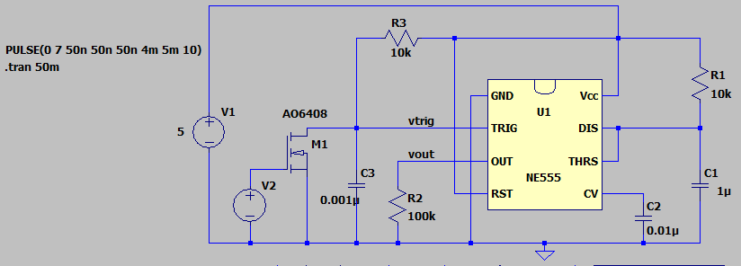
It is not noisy at all. You just had it connected incorrectly. Notice how this time you are not connecting pin 2 and pin 6 together as you did in your original design. I have simulated the device along with two ‘button presses’ which includes contact bounce and it works just fine.
I would suggest, any time that you’re incorporating new devices into your design to read the datasheet carefully and simulate the circuit so that you gain insight as to how the circuit operates as well as to verify its operation based on sound theory.
Connect the circuit as shown here. Note that the top plot in red represents the input to the TRIG input pin - button signal with contact bounce. The blue trace represents the voltage on C1 (vcap). Note that when its voltage reaches (2/3)Vcc, the output returns to its normal state. The bottom plot (green), represents the output of the 555 chip. The on time of the output pulse lasts for 1.1 x R1 x C1 (from the datasheet) and this value should be much greater than the expected contact bounce duration to avoid false triggering.
Notice that the moment the TRIG input reads the first falling edge, the output changes state and the capacitor C1 begins to charge. As mentioned above, once it reaches (2/3)Vcc, the output goes back to its original state.
In the circuit simulation, you can ignore the two chips on the left-hand side. They are just used to simulate the toggling of the switch twice along with contact bounce is all. Focus on the circuit on the right hand side and use it as a reference as to how to connect your circuit (you will have to calculate the values for C1 and R1 that suits your specific design requirements).
If you have not already done so, download LTspice and get familar with the tool. It comes in very handy. Another good tool is SIMetric SIMPLIS Elements. Both are good for simulating circuits - one has component libraries the other doesn’t (vice versa) along with different capabilities.